Following is an object-oriented analysis of concepts involved in representing circuit schematics and of flattening them into a form suitable for printed-circuit board layout.
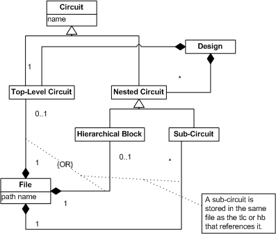
A design represents one entire schematic capture. It is composed of one top-level circuit and 0 or more nested circuits. A top-level circuit is stored in a file of its own (at most one tlc per file).
There are two types of nested circuits. Hierarchical blocks are stored in a file of their own (one per file). Sub-circuits are stored inside the file of the TLC or HB that nests them (possibly recursively). Note that sub-circuits may only be referenced from circuits stored in the same file as itself. Note also that nested circuits may not create a cycle.
When opening a file, the file that is opened becomes the top-level circuit. All nested circuits are automatically opened (at least virtually). Thus the difference between a top-level circuit and a hierarchical block is chiefly one of context.
All types of circuit have a name. The name of a tlc or hb is derived from the filename (stripping path and suffix). The name of an sc is whatever name it is given at creation.
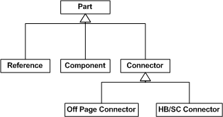
Parts are the things that a designer places on a schematic. The basic type of part is a component. That could be a resistor, a transistor, and AND gate from a TTL logic chip, and so on.
Special kinds of parts that do not correspond to circuit elements are used to connect circuits to one another. A reference is a type of part that is used to connect a parent circuit to a sub-circuit. HB/SC connectors are used within the nested circuit to define the connection points from the parent (see Nested Circuits below). Off-page connectors are used to make nets cross pages within a circuit (see Pages and Nets below).
These concepts will be explained at greater length below.
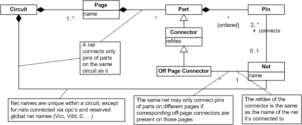
Every circuit contains at least one page, and possibly more. Each page has a page name. When a circuit has only one page, we generally suppress the notion of page. Every time a new circuit is created, it is auto-assigned a page named "1".
A designer places parts onto pages. All parts have pins (some of which are sometimes hidden on the schematic - e.g., in the case of power and ground for digital parts - these pins and their associated wires just clutter the diagram). Pins are connected to other pins using named nets. A net always connects two or more pins. Pins may be unconnected. The pins within a part are always given in a particular order during import and export. The order is defined by the pin order of the type of part from which it came (see Symbols).
Within any circuit, the net names are entirely unique (in fact, if two nets are named to be the same thing, we fold them into the same net). This is for the most part true on pages as well with one exception. The same net may appear on multiple pages if and only if the nets are connected to at least one "Off-Page Connector" of the same name as that net on each page the net appears.
Nets within different circuits in the same design may have the same base name, and are not considered connected. The one exception to this rule (and the off-page rule) is that there are six special "global" nets:
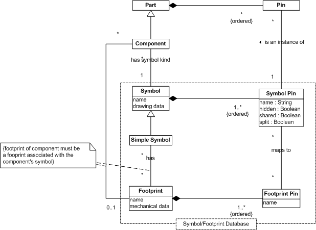
Certain parts represent the actual components of an electrical circuit rather than just being used to connect circuits and pages to one another. Every such component has a symbol associated with it. This symbol is stored in a database. There are two types of symbols: simple symbols and symbols used for multi-section parts. We shall only consider simple symbols at present. The other type will be dealt with in Multi-Section Parts. Symbols have a symbol name, and data describing how to draw the symbol on a schematic.
All symbols define a set of symbol pins. Each symbol pin has a name (not necessarily unique). The pins of a component are instances of these symbol pins. (i.e., whenever a component corresponding to a given symbol is placed on a schematic, the pins of that component are instantiated from the symbol's pins). Symbol pins may be designated as hidden meaning that neither they nor the segments of the nets that connect to them are to be drawn on the schematic. Symbol pins are ordered for the purposes of ordered lists during imports and exports.
Simple symbols generally have an associated footprint. A footprint contains all the information about the physical size and shape (in 3D) of the actual component (the mechanical data). Footprints have footprints pins that are mapped to symbol pins. Footprint pins are ordered for the purposes of ordered lists during imports and exports. Certain symbols may not have a footprint. These types of symbols may not be laid out on a PCB.
Other symbols may have several associated footprints to choose from. This is the case when one specific type of electrical component is available in several different packages (either from the same manufacturer or from different ones). In such a case, the component (which is the "instance" of a symbol) must specify which of the footprints it uses. As well, the symbol pin in this case will map to several footprints pins owned by each of the allowed footprints. Note the constraint (not shown) that a symbol pin may only map to footprint pins on one of the footprints associated with the symbol.
The "split" symbol pin attribute applies in the case where one symbol pin maps to several footprint pins on the same footprint. This type of mapping may only occur when the split attribute is set. This is done in cases where one pin on the device cannot handle all the power demands, and multiple pins must be used to prevent meltdown.
Note that the entire situation is complicated by devices whereby a single package (a single footprint) contains multiple components. This complication is dealt with below in the section Multi-Section Parts. The symbol pin attribute "shared" applies to this case and will be discussed below.
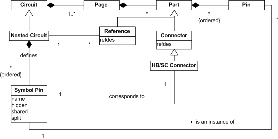
Nested circuits are connected to their parent (referencing) circuit using a special kind of part called a reference. As for any other kind of part, references define 1 or more pins. In the case of references, these pins correspond to the connection points into the nested circuit.
For component parts, the pins are instantiated from the symbol pins of the symbol kept in the shared database of symbols and footprints. For reference parts, the corresponding symbol pins are defined by the nested circuit itself. In particular, a symbol pin is defined on a nested circuit when that nested circuit contains an hb/sc connector. In this case, the refdes of the connector is the same as the name of the symbol pin. The symbol pins defeined by the HB/SC Connectors are assigned an arbitrary order, useful during import and export. A nested circuit with no symbol pins is possible, though only useful as a temporary measure.
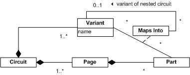
Each circuit has one or more variants (e.g., for representing slightly different circuits that for the most part are identical). When a circuit has only one variant, we generally suppress the notion of variant. Every time a new circuit is created, it is auto-assigned a variant named "Default".
Every part on a page has a "variant status" which indicates in which variants of a circuit that part appears. If the part is a reference to a nested circuit, then in addition to specifying if the reference part is present or absent in the variant, we must additionally state which of the variants of the nested circuit is to be used.
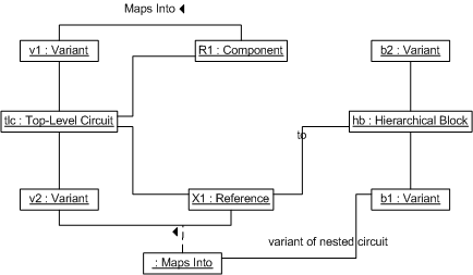
The object diagram below illustrates an example.
Top-level circuit tlc contains two parts:
a resistor R1 and a reference to the hierarchical block hb.
(Note: the page level was omitted for simplicity).
Tlc has two variants, v1 and v2. Hb also has two variants, called b1 and b2. The resistor appears in variant v1, but not in variant v2. The reference to the hierarchical block appears in v2, but not in v1. Furthermore, saying that hb is referenced from v2 of tlc is not sufficient. We must additionally state which of hb's two variants is mapped in. In this case, the link to the association object "Maps Into" indicates that it is variant b2 of hb that is mapped into variant v2 of tlc.
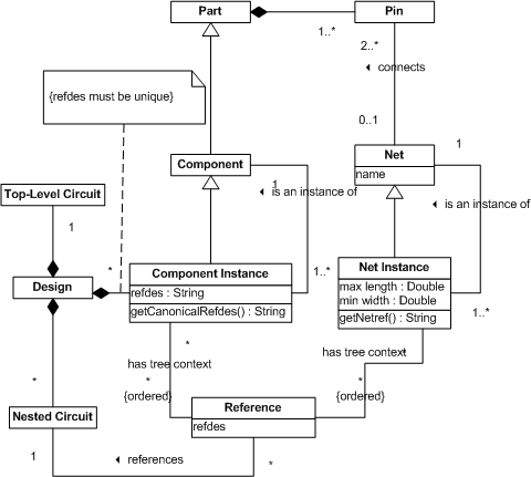
So far, we have discussed the notions of components and of nets. Two additional concepts that are important are those of instances of components and of nets.
A given nested circuit may be re-used multiple times in the same design. Each use of the nested circuit is associated with the path of references used to get to it. Every component on the re-used nested circuit therefore has several component instances associated with it. Each component instance corresponds to one use of that component within each use of the nested circuit.
We associate with each component instance a refdes. In this manner components may be identified uniquely after being transferred to PCB without a cumbersome pathname. This is important, as the component's refdes is typically silk-screened onto the board. Note that the instance refdes must be unique across the entire design. The design owns the component instances in the sense that each design must maintain a "mapping table" used to map (conceptual) instances of components into their refdes. The composition association between Design and Component Instance is, in effect, this mapping table.
These concepts are illustrated in the object diagram shown below.
In this example, we have a tlc with 2 references to the same hb
which itself has two references to the same sc.
The sc contains a lone (nameless) resistor.
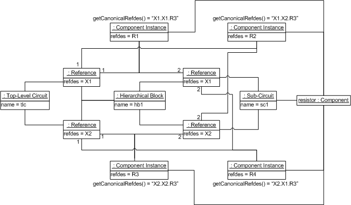
Refdes are only associated with instances of resistors. There are four instances of this resistor, named R1, R2, R3, and R4, according to the four paths through the reference tree to access them. When transferred to PCB, there will be four resistors placed on the board.
The situation is similar with nets. However, because the names of nets are not silk-screened onto PCBs, we need not name them concisely. Thus a Net Instance has an operation which can generate a "netref" by prepending the '.' separated path of the references to the net's name. A similar operation is used to generate a "canonical refdes" for component instances. The only exception to this rule is that the 6 global nets have a netref the same as the net's name. Each instance of a net also has associated data. One datum is the minimum trace width for the corresponding PCB copper trace (in cases where nets carry a lot of power and we don't want the copper melting). The second is the maximum trace length (in cases where nets carry high-frequency information and overly-long traces would lead to interference problems).
One can additionally introduce the concepts of circuit instances, page instances, pin instances and so on analogous to net instances. However, these classes are much less important that component instances and net instances as no new information is carried with them.
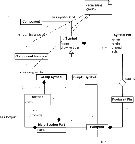
Previously in Symbols we discussed the symbol/footprint database, however we left off a discussion of multi-section parts until now. A multi-section part corresponds to a device whereby a single package (a single footprint) contains multiple components.
There are actually two types of symbols. the regular simple symbol with which we are already familiar, and a group symbol associated with multi-section parts. A group symbol represents a particular function within a multi-section part. For example, an AND gate. Multi-section parts have at least one group symbol, and may have more. Each group has one or more sections on the multi-section part. The section names must be unique within a given multi-section part. The sections are ordered within a multi-section part for the sake of file imports and exports.
Specific sections are assigned to component instances. There is a constraint that a section may only be assigned to a component instance if its component's symbol is a group symbol containing that section.
In the case of a multi-section part, the mapping of symbol pin to a footprint is more complex than in the simple case. The group symbol specifies a number of symbol pins. If the group has more than one section, and the symbol pin is not shared, there will be more than one footprint pin mapped from the symbol pin. The section that is assigned to the component instance will determine which of the footprint pins the part pin maps to.
Note however that there may be more than one footprint pin associated even with a regular symbol pin (this is the case when one pin cannot handle the power by itself). This can also happen on multi-section parts (however the UML is not affected because a '*' is a '*', whatever the reason for it).
The concept of a shared pin is one that applies to multi-section parts only. This is done when multiple sections all get power and ground from the same pins. In this case, there might be more than one symbol pin mapping to exactly one footprint pin (one per group). Pins may only be shared between sections of the same multi-section part. Not that it is possible (and in fact likely) that the concept of shared pins and split pins are combined.
To illustrate these ideas, we include an object diagram below.
In this example, a multi-section part contains two sections,
A and B.
Both sections are AND gates.
The symbol for the AND gate has 5 pins: 2 inputs, an output, and power and ground.
The power and ground pins are shared between sections A and B, and are hidden
on the schematic.
The footprint is the popular DIP8 package (dual in-line pin – 4 pins per side).
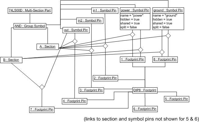
The 3-way links in the diagram correspond to the "Maps To" association. (2 of these links are not shown in order to simplify the diagram). Note how each link maps a symbol pin to a footprint pin section by section. Consider the symbol pin "out". In section A it maps to footprint pin 4. In section B it maps to footprint pin 7. Now consider the shared power pin. In both sections A and section B it maps to footprint pin 1. This is only allowed for shared pins. Were this a split shared pwoer pin, each section would map the symbol pin to multiple footprint pins. PCB layout would route copper to all of those pins to prevent pin meltdown.
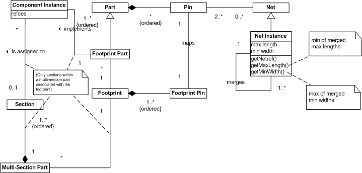
To transfer to PCB layout is it required to collapse multi-pages, flatten out all hierarchy, merge nets, and replace components by their footprints. To facilitate this, we model a Footprint Part that is a direct instantiation of a Footprint into a netlist suitable for transfer to PCB. This is a kind of part, so it has pins. These pins map 1-to-1 with the pins on the Footprint with which the Footprint Part is associated. These pins are connected to one another via net instances, named according to their generated netref. The Footprint Part also maintains an association with the Component Instance that it implements. In the case of multi-section parts, there will be several such component instances. The order in which they are listed (in import and export files) must correspond to the order in which the sections are given in the corresponding multi-section part. If a section is not mapped, a place-holder will be used.
When net instances are merged, the lowest numbered (or alphabetical) net at the highest level in the hierarchy will name the collapsed instance net. The corresponding collapsed instance net will have the minimum of the max lengths, and the maximum of the min widths of the constituent instance nets.
Version Control Information:
$Author: Dave $
Last Modified: $DateTime: 2004/10/26 14:38:13 $
$File: 407/a1/index.html $
$Revision: #5 $