
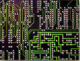
| Circuit Schematic | Printed Circuit Board | |
|---|---|---|
| | top |
| bottom |
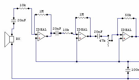
Write the OOA part of a specification for a circuit schematic entry and printed circuit board layout toolset which includes variant support. Variant support allows the user to draw one schematic for situations where circuits exist in variants: for example, an American 110V power supply and a European 220V power supply.
You are to hand in an OOA with accompanying written text in the style of the OOA part of the example given on the course web page. Assignment 2 will have you design an object-oriented program based on this OOA. Base your OOA on the following statement which describes the situation. Note, this statement is neither complete nor consistent. You may pose followup questions during lecture or on the course newsgroup. To maintain consistency, rely only on information given by Professor Penny. Be sure to account for all of the various complexities/subtleties in your OOA.
A complete circuit design is composed of a hierarchically-organized set of circuits. There is one top-level circuit, and it references, either directly or indirectly, all other (nested) circuits. As well, a circuit at any level in the hierarchy may be composed of multiple pages for ease of presentation.
There are two types of nested circuits: sub-circuits and hierarchical blocks. The only difference is that sub-circuits are stored in the same file as their referencing circuit, and may not be (directly) referenced from outside that file. Hierarchical blocks and top-level circuits are stored in their own file. Nested circuits may themselves nest circuits. Cycles are not allowed.
Each page of each circuit contains parts. A part may either be a component or a reference. A component corresponds to a real component, such as a resistor, a transistor, a diode, an IC, and so on. A reference is a connection to a nested circuit. All parts have a symbol, which is how the part is represented on the schematic. Symbols have pins, which are connection points to that symbol. Two or more symbol pins on the same page of the same circuit are connected to one another via a named "net".
There are special one-pin components which are used to connect nets across pages. These are called "off-page connectors". As well, another special kind of component is used to define the symbol pins for a nested circuit and to connect the sub-circuit parts to the circuit that references it. These are called "HB/SC connectors".
Every instance of use of a component (components in nested circuits may have several use instances) is assigned a design-wide unique identifier called a "refdes" (for "reference designator"). Likewise for all nets, but called the "netref".
All components have a footprint, which is how the component physically appears when placed on a printed-circuit board. A footprint includes all the mechanical information (i.e., 3D shape and material). Footprints have footprint pins, which are the real electrical connection points that get soldered to printed circuit boards. Symbol pins map to footprint pins.
Certain components are individual sections of a multi-section part, meaning that several parts (not necessarily all of the same type) are implemented in the same footprint package. (e.g., a TI 74LS00D QUAD 2-INPUT NAND GATE IC). In this case, certain symbol pins that appear on each symbol are shared (such as power and ground). Prior to transfer to PCB, an optimizing algorithm is run that packs compatible sections efficiently into chips so as to minimize the number of chips used. Note that if in the schematic shared pins on two different parts are not connected electrically, those parts may not be merged. The result of the packing is associated with the component instance, not the component itself, and must be stored so as to provide traceability between the part on the schematic and the part on the PCB layout for cross-probing purposes. ("cross-probing" is identifying a part on either the PCB board or the circuit schematic, and hilighting all instances of that part on the other).
Certain properties are associated with instance nets as well, such as max length and min width of the associated PCB traces (necessary for high-speed applications). Because nets are connected across pages and sub-circuits, a PCB net may include several schematic nets. In such a case, the minimum width of the PCB trace is the minimum of the schematic minimum trce widths. Likewise for maximum length.
Every circuit (whether top-level or nested) carries a set of named variants. Each part that is placed on a circuit indicates in which variant it appears. Typically, most parts will appear in all variants. If a reference appears into a certain variant, we must additionally state which variant of the referenced nested circuit is the one that is mapped.
The program you will eventually write will read schematics into memory from text files, flatten out all references to nested circuits, optimally consolidate instance components and nets, and output a consolidated minimal representation for input to a PCB layout toolset that allows for cross-probing back to schematic entry. Because schematic parts/nets are so similar to PCB parts/nets, your OOA should be sufficiently general to represent both. Eventually, when you get to writing the program, the OOA will be transformed into classes, and these classes can then be used to represent both the input and the output. More details will follow when A2 is handed out October 25th.
Good luck!